


Hello! I am Kevin Ferri. Currently I am a Ph.D. candidate in Materials Science and Engineering at Penn State University.
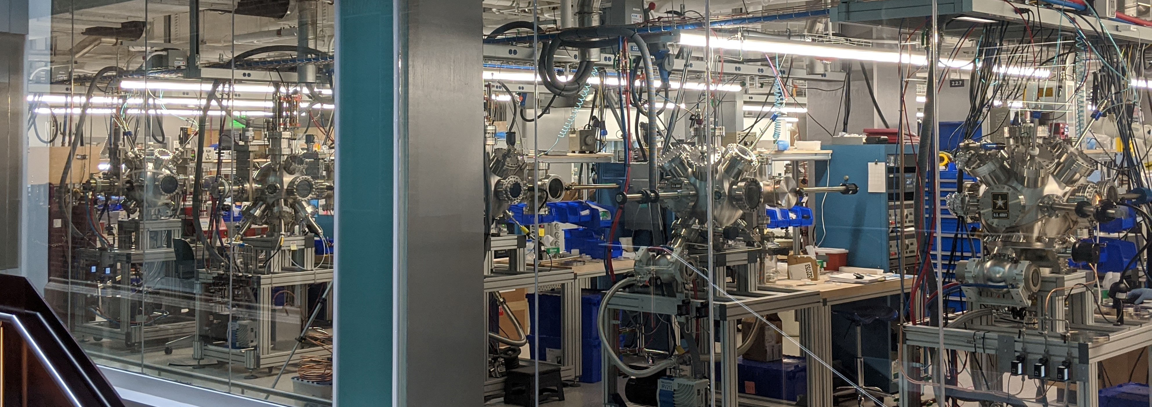
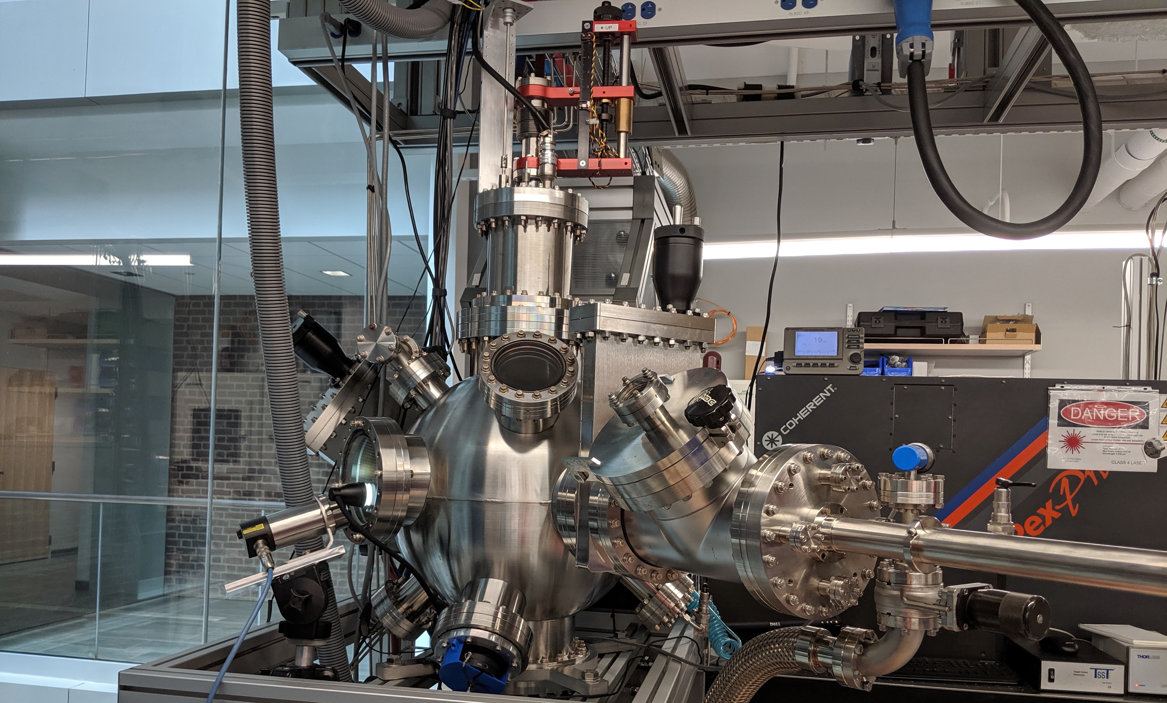
I have been a materials scientist for 5 years primarily focusing on thin films via physical vapor deposition. Throughout my research career, I have applied this knowledge to develop processes across a wide range of materials systems and techniques.
Currently I have two main projects.
The first utilizes thin film geometries to simulate bulk varistor grain boundaries and study the correlation between phase formation and electronic behavior, something which has been historically challenging for the bulk varistor community. My second project focuses on substituting ZnO with high percentages of MgO near the wurtzite to rocksalt transition in an effort to produce hexagonal Zn1-xMgxO which is ferroelectric.
I will be defending my doctorate on the emergent dielectric and conducting phenomena at phase boundaries and physical interfaces in ZnO based materials systems at the end of 2020. As my time in graduate school comes to an end, I am looking for a career which allows me to use my expertise and experience to develop new techniques and explore new and interesting materials systems.
Varistors are technologically important for their large energy handling capabilities and highly nonlinear electrical behavior when voltages above a characteristic switch field are applied. The prototypical ZnO-Bi2O3 varistor system forms electrostatic Schottky barriers at grain boundaries in response to residual Bi and other dopants left at grain surfaces during Bi2O3 segregation. While barrier heights can be modulated with formulation and defect chemistry, mechanisms by which dopant locations, defect compensation, and local phases determine varistor behavior is not completely understood. Bulk studies are challenging due to random grain boundary formation and difficulties studying individual boundaries. To circumvent these challenges in the ZnO-Bi2O3 varistor system, we use as-deposited and post heat-treated thin film ZnO-Bi2O3 prototypes to simulate bulk varistor grain boundary phase formation and investigate resulting defect chemistry. Characterizing interactions between Bi2O3 films deposited on thin film and single crystal ZnO by XRD and TEM-EDS revealed primarily Zn-out diffusion, resulting in two (Bi2O3)1-x(ZnO)x phases. Subsequently we developed a saturated front model, based on Zn-out diffusion, which correlates changes in Bi2O3 thickness to phase evolution. Next, we explored post heat-treated (Mn:ZnO)-Bi2O3 stacks. Lastly, we began correlating as-deposited Bi2O3 phases with resulting electrical behavior and found on average, a 12x difference between nonlinear coefficients for γ*- and β*-BZO.
Ferri, K., Paisley, E., DiAntonio, C., Han, S-W., Chu, R., Maria, J-P. Investigation of phase evolution within ZnO-Bi2O3 varistors utilizing thin film prototypes. Submitted
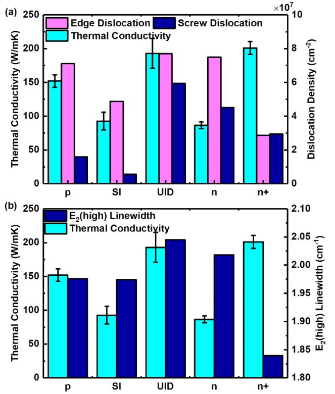
Gallium nitride (GaN) has emerged as one of the most attractive base materials for next-generation high-power and high-frequency electronic devices. Recent efforts have focused on realizing vertical power device structures such as in-situ oxide, GaN interlayer based vertical trench metal-oxide-semiconductor field-effect transistors (OG-FETs). Unfortunately, the higher power density of GaN electronics inevitably leads to considerable device self-heating which impacts device performance and reliability. Halide vapor phase epitaxy (HVPE) is currently the most common approach for manufacturing commercial GaN substrates used to build vertical GaN transistors. Vertical device structures consist of GaN layers of diverse doping levels. Hence, it is of crucial importance to measure and understand how the dopant type (Si, Fe, and Mg), doping level, and crystal quality alter the thermal conductivity of HVPE-grown bulk GaN. In this work, a steady-state thermoreflectance (SSTR) technique was used to measure the thermal conductivity of HVPE-grown GaN substrates employing different doping schemes and levels. Structural and electrical characterization methods including x-ray diffraction (XRD), secondary-ion mass spectrometry (SIMS), Raman spectroscopy, and Hall-effect measurements were used to determine and compare the GaN crystal quality, dislocation density, doping level, and carrier concentration. Using this comprehensive suite of characterization methods, the interrelation among structural/electrical parameters and the thermal conductivity of bulk GaN substrates was investigated. While doping is evidenced to reduce the GaN thermal conductivity, the highest thermal conductivity (201 W/mK) is observed in a heavily doped Si-doped (1-5.00 x 1018 cm3) substrate with the highest crystalline quality. This suggests that phonon-disclocation scattering dominatnes over phonon-impurity scattering in the tested HVPE-grown bulk GaN substrates. The results provide useful information for designing thermal management solutions for vertical GaN power electronic devices.
Song, Y., Lundh, J., Wang, W., Leach, J., Eichfeld, D., Krishnan, A., Perez, C., Ji, D., Borman, T., Ferri, K., Maria, JP., Chowdhury, S., Ryou, J., Foley, B., Choi, S. The doping dependence of the thermal conductivity of bulk gallium nitride substrates. J. Electron. Packag. 142, 041112 (2020)
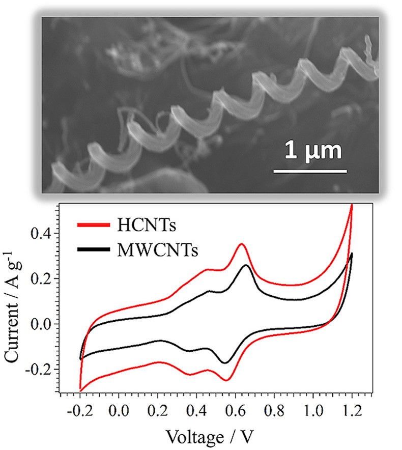
Despite their low specific surface area (500 m2 g-1) relative to that of activated carbon (1500–2000 m2 g-1), carbon nanotubes are attractive as effective electrode materials for supercapacitors. Electrodes comprised of arrays of helically coiled carbon nanotubes (HCNTs) and multi-wall carbon nanotubes (MWCNTs) were prepared and evaluated as novel electrode materials for electric double layer capacitors (EDLCs). While both types of electrodes exhibited a linear dependence on array height and a diffusion limited behavior below the 1 V s-1 scan rate, the electrodes comprised of HCNT arrays exhibited better performance. Freestanding HCNT and MWCNT buckypapers were also prepared and used as electrodes, and the former showed a higher energy density relative to the latter with no loss in its power density and capacity fade. Collectively, this study concludes that HCNTs are well suited as binder-free electrodes that can be augmented with electroactive polymers for improved EDLC performance.
Childress, A., Ferri, K., Rao, A. Enhanced supercapacitor performance with binder-free helically coiled carbon nanotube electrodes. Carbon. 140, 0008-6223 (2018)
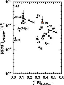
Time domain thermoreflectance (TDTR) and frequency domain thermoreflectance (FDTR) are common pump-probe techniques that are used to measure the thermal properties of materials. At elevated temperatures, transducers used in these techniques can become limited by melting or other phase transitions. In this work, time domain thermoreflectance is used to determine the viability of HfN thin film transducers grown on SiO2 through measurements of the SiO2 thermal conductivity up to approximately 1000 K. Further, the reliability of HfN as a transducer is determined by measuring the thermal conductivities of MgO, Al2O3, and diamond at room temperature. The thermoreflectance coefficient of HfN was found to be 1.4 × 10⁻⁴ K-1 at 800 nm, one of the highest thermoreflectance coefficients measured at this standard TDTR probe wavelength. Additionally, the high absorption of HfN at 400 nm is shown to enable reliable laser heating to elevate the sample temperature during a measurement, relative to other transducers.
Rost, C., Braun, J., Ferri, K., Backman, L., Giri, A., Opila, E., Maria, JP., and Hopkins, P. Hafnium nitride films for thermoreflectance transducers at high temperatures: Potential based on heating from laser absorption. J. Appl. Phys. Lett. 111, 151902 (2017)
June 2016 - Present
February 2015 - May 2016
Novermber 2013 - May 2016
January 2015 - May 2015